- 您现在的位置:买卖IC网 > Sheet目录2005 > LTC2234IUK#TRPBF (Linear Technology)IC ADC 10BIT 135MSPS SAMPL 48QFN
LTC2234
15
2234fa
APPLICATIO S I FOR ATIO
WU
UU
signal at its optimum DC level. Terminating on the trans-
former secondary is desirable, as this provides a common
mode path for charging glitches caused by the sample and
hold. Figure 3 shows a 1:1 turns ratio transformer. Other
turns ratios can be used if the source impedance seen by
the ADC does not exceed 100
for each ADC input. A
disadvantage of using a transformer is the loss of low
frequency response. Most small RF transformers have
poor performance at frequencies below 1MHz.
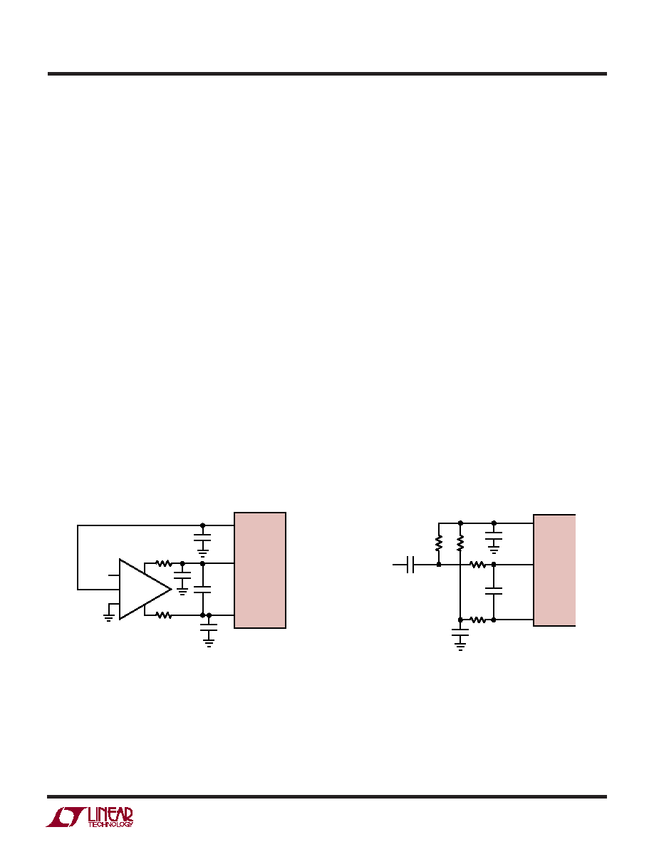
Figure 4 demonstrates the use of a differential amplifier to
convert a single ended input signal into a differential input
signal. The advantage of this method is that it provides low
frequency input response; however, the limited gain band-
width of most op amps will limit the SFDR at high input
frequencies.
Figure 5 shows a single-ended input circuit. The imped-
ance seen by the analog inputs should be matched. This
circuit is not recommended if low distortion is required.
The 25
resistorsand12pFcapacitorontheanaloginputs
serve two purposes: isolating the drive circuitry from the
sample-and-hold charging glitches and limiting the
wideband noise at the converter input. For input frequen-
cies higher than 100MHz, the capacitor may need to be
decreased to prevent excessive signal loss.
For input frequencies above 100MHz the input circuits of
Figure 6, 7 and 8 are recommended. The balun trans-
former gives better high frequency response than a flux
coupled center tapped transformer. The coupling capaci-
tors allow the analog inputs to be DC biased at 1.6V. In
Figure 8 the series inductors are impedance matching
elements that maximize the ADC bandwidth.
Reference Operation
Figure 9 shows the LTC2234 reference circuitry consisting
of a 1.6V bandgap reference, a difference amplifier and
switching and control circuit. The internal voltage refer-
ence can be configured for two pin selectable input ranges
of 2V (
±1Vdifferential)or1V(±0.5Vdifferential).Tyingthe
SENSE pin to VDD selects the 2V range; tying the SENSE
pin to VCM selects the 1V range.
The 1.6V bandgap reference serves two functions: its
output provides a DC bias point for setting the common
mode voltage of any external input circuitry; additionally,
the reference is used with a difference amplifier to gener-
ate the differential reference levels needed by the internal
ADC circuitry. An external bypass capacitor is required for
the 1.6V reference output, VCM. This provides a high
frequency low impedance path to ground for internal and
external circuitry.
Figure 4. Differential Drive with an Amplifier
Figure 5. Single-Ended Drive
25
25
AIN
+
AIN
–
12pF
2.2
F
3pF
VCM
LTC2234
2234 F04
–
+
CM
ANALOG
INPUT
HIGH SPEED
DIFFERENTIAL
AMPLIFIER
AMPLIFIER = LTC6600-20,
"LT1993", ETC.
25
0.1
F
ANALOG
INPUT
VCM
AIN
+
AIN
–
1k
12pF
2234 F05
2.2
F
1k
25
0.1
F
LTC2234
发布紧急采购,3分钟左右您将得到回复。
相关PDF资料
LTC2237IUH#TRPBF
IC ADC 10BIT 40MSPS 3V 32-QFN
LTC2239CUH#PBF
IC ADC 10-BIT 80MSPS 3V 32-QFN
LTC2240CUP-12#PBF
IC ADC 12BIT 170MSPS 64-QFN
LTC2240IUP-10#PBF
IC ADC 10BIT 170MSPS 64-QFN
LTC2241IUP-10#PBF
IC ADC 10BIT 210MSPS 64-QFN
LTC2242IUP-10#PBF
IC ADC 10BIT 250MSPS 64-QFN
LTC2245IUH#TRPBF
IC ADC 14BIT 10MSPS 3V 32-QFN
LTC2249IUH#TRPBF
IC ADC 14BIT 80MSPS LP 32-QFN
相关代理商/技术参数
LTC2234UK
制造商:LINER 制造商全称:Linear Technology 功能描述:10-Bit, 135Msps ADC
LTC2236
制造商:LINER 制造商全称:Linear Technology 功能描述:14-Bit, 80Msps Low Power 3V ADC
LTC2236CUH
制造商:LINER 制造商全称:Linear Technology 功能描述:10-Bit, 65/40/25Msps Low Noise 3V ADCs
LTC2236CUH#PBF
功能描述:IC ADC 10-BIT 25MSPS 3V 32-QFN RoHS:是 类别:集成电路 (IC) >> 数据采集 - 模数转换器 系列:- 标准包装:1 系列:microPOWER™ 位数:8 采样率(每秒):1M 数据接口:串行,SPI? 转换器数目:1 功率耗散(最大):- 电压电源:模拟和数字 工作温度:-40°C ~ 125°C 安装类型:表面贴装 封装/外壳:24-VFQFN 裸露焊盘 供应商设备封装:24-VQFN 裸露焊盘(4x4) 包装:Digi-Reel® 输入数目和类型:8 个单端,单极 产品目录页面:892 (CN2011-ZH PDF) 其它名称:296-25851-6
LTC2236CUH#TRPBF
功能描述:IC ADC 10BIT 25MSPS 3V 32-QFN RoHS:是 类别:集成电路 (IC) >> 数据采集 - 模数转换器 系列:- 标准包装:2,500 系列:- 位数:16 采样率(每秒):15 数据接口:MICROWIRE?,串行,SPI? 转换器数目:1 功率耗散(最大):480µW 电压电源:单电源 工作温度:-40°C ~ 85°C 安装类型:表面贴装 封装/外壳:38-WFQFN 裸露焊盘 供应商设备封装:38-QFN(5x7) 包装:带卷 (TR) 输入数目和类型:16 个单端,双极;8 个差分,双极 配用:DC1011A-C-ND - BOARD DELTA SIGMA ADC LTC2494
LTC2236CUHPBF
制造商:Linear Technology 功能描述:ADC 10-Bit 25Msps Low Noise 3V QFN32
LTC2236IUH
制造商:LINER 制造商全称:Linear Technology 功能描述:10-Bit, 65/40/25Msps Low Noise 3V ADCs
LTC2236IUH#PBF
功能描述:IC ADC 10-BIT 25MSPS 3V 32-QFN RoHS:是 类别:集成电路 (IC) >> 数据采集 - 模数转换器 系列:- 标准包装:1 系列:microPOWER™ 位数:8 采样率(每秒):1M 数据接口:串行,SPI? 转换器数目:1 功率耗散(最大):- 电压电源:模拟和数字 工作温度:-40°C ~ 125°C 安装类型:表面贴装 封装/外壳:24-VFQFN 裸露焊盘 供应商设备封装:24-VQFN 裸露焊盘(4x4) 包装:Digi-Reel® 输入数目和类型:8 个单端,单极 产品目录页面:892 (CN2011-ZH PDF) 其它名称:296-25851-6